


Maskless Lithography System - Speed
System Composition
A DMD-based maskless lithography system typically comprises several key components: a light source module, a beam homogenization module, a DMD module, a projection module, a motion stage module, and software. These modules work together with high efficiency and precision to enable rapid, maskless lithography of high-resolution patterns.
Workflow
The host computer transmits pattern data to the DMD module, which displays the corresponding pattern. Light reflected from the DMD—carrying the pattern information—passes through a series of optical elements and illuminates the substrate, thereby transferring the pattern. The coordinated operation of the high-precision motion stage ensures the accurate stitching of different exposure areas, ultimately enabling the dynamic exposure of large-scale, complex patterns.
Key Features
- Flexible, maskless design
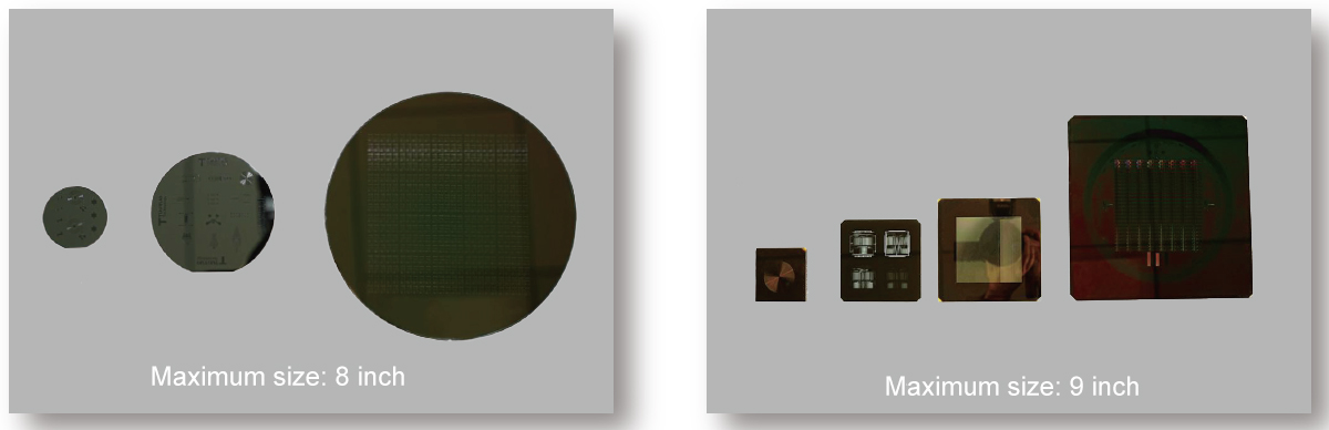
- Processing precision up to 400 nm
- Processing speed up to 1200 mm²/min
- Processing area up to 4 m²
- Grayscale lithography up to 4096 levels
Applications:
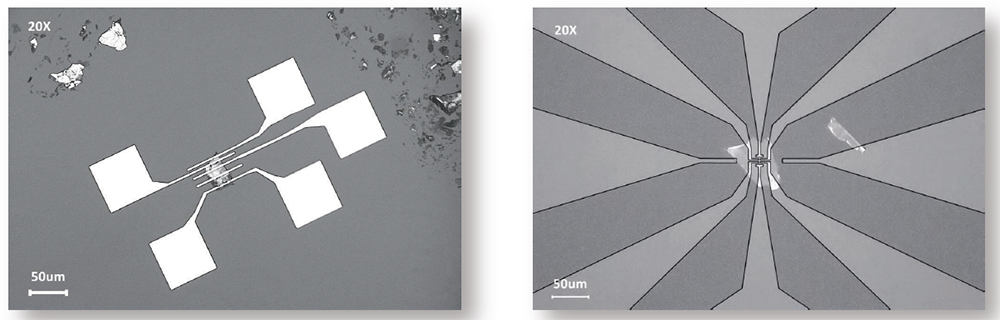
2D Materials
Proprietary "guide light" and "direct writing" functions enable the direct patterning of electrodes onto target 2D materials with flexibility and high efficiency.
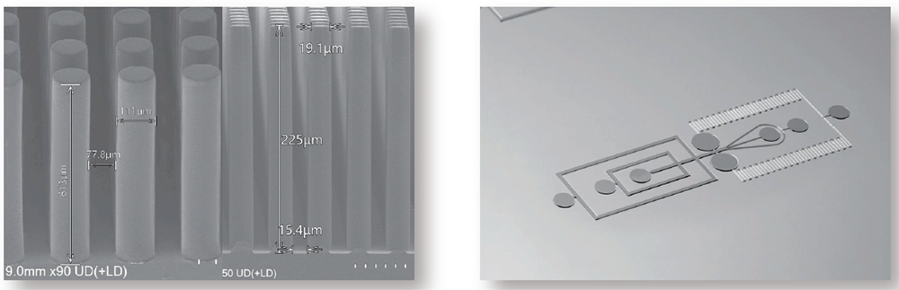
Microfluidics
Maskless lithography systems can fabricate high-aspect-ratio (10:1) structures, offering high precision and flexibility for microfluidic chip manufacturing; they are widely used in fields such as single-cell analysis and sensor development.
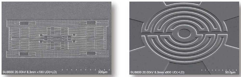
MEMS
Maskless lithography is widely applied in MEMS, enabling the high-precision fabrication of micron-scale patterns and the processing of complex structures through multi-layer alignment.
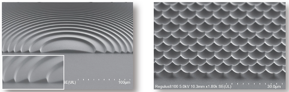
Microlenses
Grayscale lithography allows for precise control over surface topography, enabling the creation of complex diffractive structures such as gratings, Fresnel lenses, and microlenses.
Optical Diffractive Devices
In optical modulation devices, grayscale lithography utilizes precise control of exposure intensity to fabricate highly detailed optical microstructures, optimizing light wave modulation and transmission characteristics.
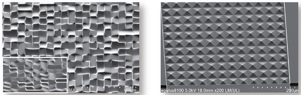
Relief Structures
For anti-counterfeiting relief structures, grayscale lithography employs fine control of exposure intensity to create high-precision 3D microstructures, increasing the complexity and difficulty of replicating the anti-counterfeiting marks.
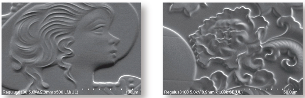
Metasurfaces
Lithography processes enable the precise fabrication of micro- and nano-scale structures for metasurfaces, allowing for the fine manipulation of light waves and the modulation of optical properties such as specific wavelengths and polarization.
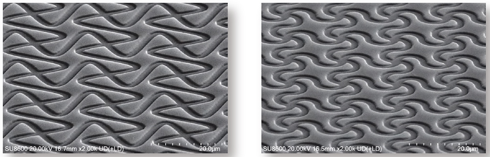
Quantum Optics
In the field of quantum optical waveguides, lithography processes enable the precise etching of micro- and nano-scale waveguide structures, facilitating the transmission and manipulation of quantum states and advancing quantum information processing and transmission technologies.
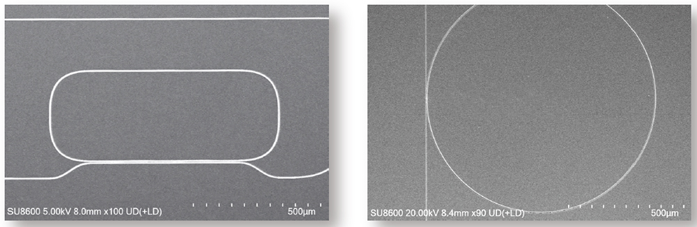
Photomask Fabrication
High-speed (up to 1200 mm²/min) maskless lithography systems are suitable for the small-batch, customized production of photomasks, reducing reliance on external suppliers and shortening design iteration cycles.
Technical specification
| Model | DXMLS-S1 | DXMLS-S2 |
| Feature size | 1.0 um | 0.5 um |
| Minimum equal line/space | 2.0 μm | 0.5 μm |
| Lithography efficiency | Shot 1: 1000 mm²/min Shot 2: 2500 mm²/min |
Shot 1: 75 mm²/min Shot 2: 300 mm²/min Shot 3: 1200 mm²/min |
| Overlay accuracy | 500 nm | 250 nm |
| (5 mm x 5 mm) | 1000 nm | 500 nm |
| Overlay accuracy | LD:405 nm / 375 nm | |
| (50 mm x 50 mm) | Supported | |
| Light source* | Optional | |
| Motorized objective switching | 3 mm × 3 mm (minimum), 200 mm × 200 mm (maximum) | |
| Grayscale lithography | 0-10 mm | |
| Sample size | GDS、DWG、DXF | |
| Sample thickness | 1700 mm * 1300 mm * 1950 mm | |
| Data format | 1400kg | |
| Main unit dimensions | Total footprint: 2.7 m × 2.3 m Power: 2.4 kW Temperature: 20–26°C Humidity: 40–60% RH Power supply: 220 V ±5%, 50 Hz ±1 Hz, 16 A |
|
Maskless Lithography technology employs a Digital Micromirror Device to control the angles of micromirrors, enabling the rapid formation of images or lithographic patterns on material surfaces via a projection system. Controlled by electrical signals, these micromirrors precisely adjust their reflection angles to project laser or other light sources onto specific locations.
